Schematic diagram of both the lead compensator and the lag compensator. G c s s 00345 s 1923 4 10 7 s 2.

1 Design A Phase Lead Cascade Compensator For The Chegg Com
For 20 OS ƺ0456 Recall𝜉 𝑀𝑝100 𝜋2 2𝑀𝑝100.
. Ii Time constant is greater than 1s. Design a lead of lag compensator so that the following specifications are satisfied. A unity feedback control system has an open loop transfer function G S K S S24S13Sketch the root locus 5.
D Design a lead compensator to meet the following specs. The phase margin is no less than 50circ. The root-locus approach to design is very powerful when the specifications are given in terms of time- domain quantities such as damping ratio undamped natural frequency desired dominant closed-loop poles maximum overshoot rise time settling time.
Show activity on this post. I ts 04 sec. Lead compensator design Consider a system Analysis of CL system for Cs1 Damping ratio Damping ratio ζζ05 Undamped natural freq.
Find the value of K so that the damping ratio of the closed loop system is 05. Lead Compensation Techniques Based on the Root-Locus Approach. An UFB system has Gs 10 𝑠𝑠1 Design Lead Compensator for the following specification e ss 20sec Phase Margin 50 deg.
𝐺𝑐 𝐾𝑐𝛼 𝑇 1 𝛼𝑇 1 𝐾𝑐. Given a unity feedback system where 1 4 s s. ωn4 rads Cs Gs Controller Plant Re Im Desired pole CL pole with Cs1.
𝐺 𝐾 50 120 Design a lead compensator for the system in example one to meet the following specifications. Design a Lead-Lag compensator for the system G s1 s s4 s10 To meet the following specifications Steady state error to a step input is 0 Steady state error to a ramp input is less than 01 Phase margin 25 deg - 0125. First of all we need to find the closed loop bandwidth to meet the transient response requirement OS20 Ts 02s.
A Draw the Bode plot of the uncompensated system and calculate the phase and gain margins of the system. Desired dominant closed-loop poles. Design a lead compensator so that the closed loop system meets the following specifications i Velocity error constant is greater than 10s.
Sketch the root locus of the system whose open loop transfer function is G S K S S2 S4. The gain crossover frequency is at least 12 rads. From the settling time spec we see that the real part of.
The steady-state error due to a unit-step disturbance input Ds is less that or equal to 5. Required for Root Locus The closed loop TF. Consider a system whose open loop transfer function is given by 13 1.
Answer to Solved Design a Lead-Lag compensator for the. OS20 Ts02s and Kv50. Electrical Engineering questions and answers.
3- We need to reshape the open loop transfer functions frequency response to meet. S K G s Design a passive lag-lead compensator using Bode diagrams to yield a 1325 overshoot a peak time of 2 seconds and Kv12. Meet the given specification.
- steady state error to a unity rate ramp is equal or less than 005 and - the damping ratio is equal or greater than 07. G_cs frac-6662s045s15. OS 20 Ts02 K v 50 2 Solution 1.
Sketch the root locus of the lead compensated system. 2- Bandwidth is related to both ƺ damping ratioand Ts settling time or Tppeak time. And Gain Margin 10dB.
Ii Mp 2. The gain crossover frequency is between 4 and 10 rads. Design a Lead compensator to place the dominant poles at the desired places while neglecting the effects of the Lag compensator.
Draw the Bode plot and find K for the following two cases. Find that value of K proportional controller. Design a lag or lead compensator Cs such that the following specifications are met.
This circuit has a transfer function of R 2 R 11 R 1 C 1 s1 R 2 C 2 s and thus provides one pole and one zero which can be placed anywhere on the negative real axisWhen the zero is closer to the origin than the pole this circuit is referred to as a lead compensator and. Desired system is K. I came up with the following compensator which gives the required specifications.
1- Phase margin is related to OS. You are required to design a lead compensator Gcs to meet the following specifications. Lead Compensation Techniques Based on the Root-Locus Approach.
AThe settling time is t s 5 sec bThe step response overshoot M p 163 cThe steady state error to a unit ramp is 10. ωωn2 rads Performance specification Damping ratio Damping ratio ζζ05 Undamped natural freq. Ηere is an open-loop transfer function and specifications for compensator design.
Due to its simplicity and And secondly by drawing root-locus plot of the uncompensated effectiveness phase lag and lead compensation is essential for system ascertain whether or not the gain adjustment alone can various frequency-based design methods especially for design yield the desired closed loop poles. The steady-state error due to a unit step disturbance is no more than 1. I defined the required poles and defined the angles according to the normal procedure of the root locus method and determined the zero and pole of the lead compensator.
What is your angle of deficiency. There is a proportional controller which will meet the transient specifications. S Compensator Controller.
Then design the Lag compensator to meet the SSE specifications. The open loop transfer function of a unity feedback control. I Gain margin equal to 6db ii Phase margin equal to 45.
2- Design of a lead compensator. The phase margin is no less than 50circ. Some Notes needed for the design.
Design a compensator which approximately meets the following specifications for unit step response. Iii Overshoot is less than 10. 3- Design of lag compensator.
The root-locus approach to design is very powerful when the specifications are given in terms of time-domain quantities such as. However it could be really challenging to deploy such compensator in real systems. Transfer function of the compensator is.
Design a lead compensator for the system to meet the following specification. Gs Plant Transfer function Lead compensation techniques based on the frequency response approach Lead compensator transfer function. 4- Design of a lead-lag compensator.

Solved You Want To Design A Lead Compensator Such That The Chegg Com
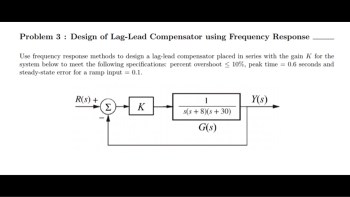
Solved Problem 3 Design Of Lag Lead Compensator Using Chegg Com
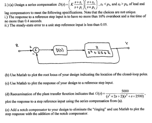
Design A Series Compensation D S Ks Z1 S Chegg Com
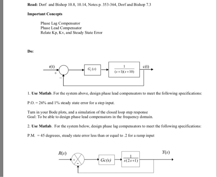
Solved Read Dorf And Bishop 10 8 10 14 Notes P 353 364 Chegg Com

How Many Lead Compensator Designs Will Meet The Chegg Com
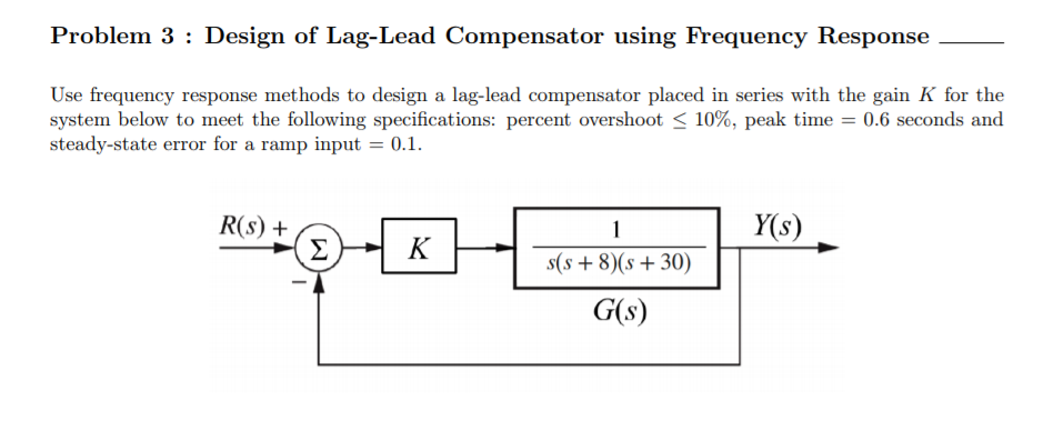
Solved Problem 3 Design Of Lag Lead Compensator Using Chegg Com
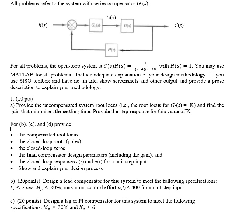
Solved All Problems Refer To The System With Series Compensator Gc S Uls R S For All Problems The Open Loop System Is G S H S With H S 1 You May Use 5 5 4 5 10 Matlab For All Problems
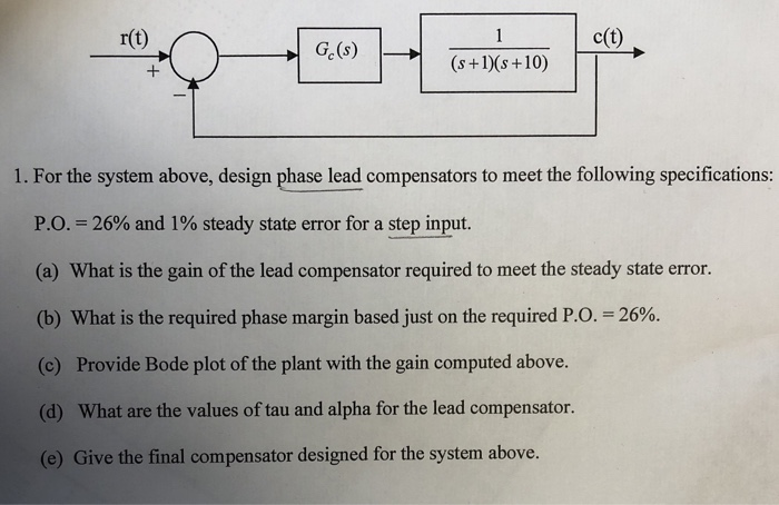
Solved C T R T 1 Go S S 1 S 10 1 For The System Above Chegg Com
0 comments
Post a Comment